Router overclocking
Real gaming router
This is part 2 of the “Real gaming router” series of blog posts. Read Part 1 / Real gaming router first.Why?
If you’ve seen part 1 of the “Real gaming router”, you know that the game performance in GTA Vice City was a bit lacking.
As a quick reminder, this is what the game looked like before any mods:
This is running at 1280x720px resolution at 16bpp color depth.
The WDR4900 is severely limited by a number of factors:
- 128 MB RAM
- Swap via USB 2.0
- Slow root filesystem (mounted via NFS over Gigabit Ethernet)
- Low CPU speed (800 MHz)
Only having 128 MB of RAM was the biggest bottleneck for sure.
GTA Vice City didn’t fit in 128 MB and having this little RAM meant that things like the video resolution needed to be cut down.
Having 2x 1920x1080px framebuffers at 32 bits per pixel was already wasting 16 MiB of RAM!
That’s an 1/8th of the total system memory! So we reduced the resolution down to 1280x720px at 16bpp.
Memory Swap (ICMAX)
The logical conclusion is: We need more RAM.
Let’s “just” buy some random DDR3 IC, swap the BGA chip and we’re good to go, right?
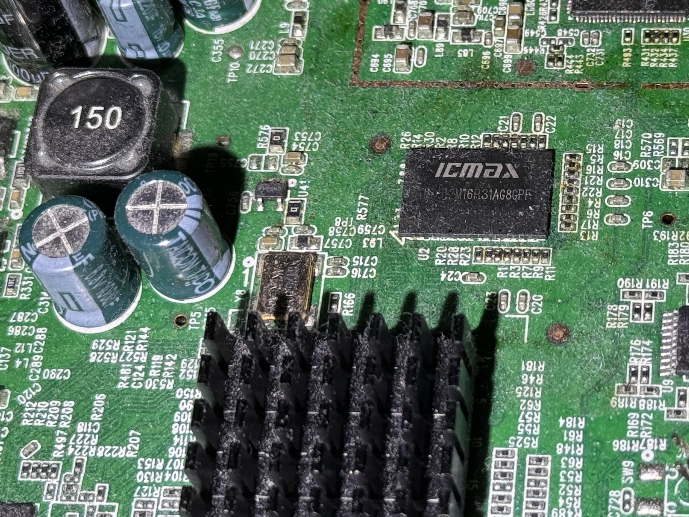
The new chip was an ICMAX IMD512M16R31AG8GPF DDR3 SDRAM IC, 8Gbit/1GByte, x16.
Of course – it wasn’t quite this easy:
After swapping the IC, the router was completely dead. Not unexpected, but a bit problematic.
How exactly do you debug DDR3 memory controller issues on a WiFi router?
This could be a number of issues:
- Bad soldering (not unlikely, it’s a somewhat challenging modification)
- Bad replacement IC (ICMAX is a relatively unknown, china-only brand with very limited reputation)
- Incompatible chip
- Incompatible settings / boot ROM
tl;dr
Things get very in-depth now. Skip to the Memory & CPU clock speed chapter if you don’t want to read the nitty-gritty details.NXP eSPI boot flow
Sidenote: CCSRBAR
In the following chapters, memory addresses will be shown. These memory addresses are physical memory addresses (before translation/MMU) and they often describe MMIO registers in the SoC. All SoC peripheral register addresses in the datasheet are specified without a special offset called the CCSRBAR.The peripheral register address space can be remapped by changing the CCSRBAR value.
The default offset on the P1014 is
0xFF700000 (which is what you’ll often see in this blog post).u-boot (in the default configuration) will remap these MMIO registers to
0xFFE00000.This warrants a closer look at the boot process of the NXP P1014 System-on-a-chip.
NXP offers the P1014 QorIQ Integrated Processor Reference Manual (NXP account required), a very in-depth 1795 page document containing a lot of details about the routers SoC.
4.6.2.3 eSPI EEPROM data structure (Page 152) describes how the SoC loads data from the SPI flash chip at startup.
NXP/Freescale have come up with quite a flexible mechanism here.
Other CPUs/SoCs will just look for a signature and load a fixed amount of code into RAM. NXPs approach was a data structure with several parameters (offset in the SPI flash, load address, execution start/jump address) and a clever trick:
The EEPROM data structure can contain a number of key-value pairs of memory addresses and data!
This allows the flash content to initialize almost any peripheral in the SoC before the data is loaded. The DDR3 memory controller, cache controller, NAND controller (and others) can be set up just by writing the appropriate values directly into the MMIO registers.
DDR3 init
TP-Link’s stock flash image uses the eSPI structure mechanism to directly configure the DDR memory controller.
The u-boot image is then directly loaded into 0x1000000 (which resides in DRAM).
This also means that broken DRAM (for whatever reason) will cause the bootloader copy and initialization to fail silently. Nothing can produce any serial output anymore and the router is dead.
| Address | Register | Content |
|---|---|---|
| FF702110 | DDR_DDR_SDRAM_CFG | 47140008 |
| FF702000 | DDR_CS0_BNDS | 00000007 |
| FF702080 | DDR_CS0_CONFIG | 80014102 |
| FF702100 | DDR_TIMING_CFG_3 | 00030000 |
| FF702104 | DDR_TIMING_CFG_0 | 00110004 |
| FF702108 | DDR_TIMING_CFG_1 | 6F6B8644 |
| FF70210C | DDR_TIMING_CFG_2 | 0FA888CF |
| […] | […] |
u-boot in SRAM
There is another approach to booting the SoC. Instead of directly configuring the DDR controller, you can also setup a feature called L2-as-SRAM. This allows the SoC to disable it’s 256 KiB of L2 data and instruction cache and instead map them to a memory area. Code can then be loaded & executed from SRAM, which can then do initialization of the memory controller and do other (more complex) functions without having any DRAM (yet).
The original u-boot on the router is a u-boot 2010.12, so it’s almost 15 years old at this point.
Modern u-boot versions like the 2024.01 release we tried to use still support the P1014 CPU.
u-boot now also includes native DDR3 memory configuration functionality.
This works by compiling u-boot with a SPL (Secondary Program Loader):
SPL is a small boot stage, which is loaded into SRAM, configures the basics (memory mappings, DDR3, etc.) and then loads the full u-boot from any other storage medium. This could even load u-boot from very complex devices like NVMe (over PCIe)!
Compiling a modern u-boot for the platform was a bit of a challenge. Finding a compatible toolchain is difficult, as GCC dropped support for PowerPC SPE in GCC 9.
We ended up doing our development in a Debian 9 VM, using the gcc-8-powerpc-linux-gnuspe toolchain.
This was problematic in itself, because Debian 9’s OpenSSL was too old for modern versions of u-boot. Things like mkimage’s cryptographic signing broke as a result.
We solved this by building OpenSSL 1.1.1w ourselves, but bootstrapping binutils and gcc on a modern Linux userland would’ve probably been a better call…
After building u-boot with a SPL enabled, we had both a u-boot.bin and a u-boot-spl.bin binary. These were missing the eSPI headers, though. Searching through NXPs SDKs and documentation brought us to a tool called boot-format.
The older sdk-v1.8.x branch still had support for our platform (while the newer ones didn’t).
The repository contains several configuration files for different platforms and hardware configurations. Those .dat files contain the raw MMIO register accesses (as described above) in text form.
Most interesting were config_ddr3_1gb_p1014rdb_667M.dat and config_sram_p1010rdb.dat. The first initializes the DDR3 memory controller directly (like the stock u-boot) and the latter configures the L2-cache as SRAM and tries to load a program into SRAM.
On the router with swapped DDR3 we needed to use the SRAM configuration to try and avoid the DRAM for now.
A flash image for the 16 MiB NOR flash was prepared like this:
#!/usr/bin/env bash
./boot_format config_sram_p1010rdb_spl.dat u-boot-spl.bin -spi spi1014.bin

truncate -s 16M spi1014pad.bin
dd if=spi1014.bin of=spi1014pad.bin bs=1M conv=notrunc

flashrom -p serprog:ip=localhost:2222 -c "S25FL128S......0" -w spi1014pad.bin
The resulting header looked like this, initializing the L2-as-SRAM and loading/executing from 0xD0000000:
SPI NOR flash hardware mods
Programming the SPI NOR flash in-circuit should be pretty easy, right?
Just keep the CPU in reset, clip a SOIC-16 clip to the IC and use any SPI flasher.
Keeping the CPU in reset was already trickier than expected, the board had a 16-pin JTAG header with the standard
JTAG RISCWATCH pinout, but none of the RESET pins were able to keep the CPU in reset.
Next to the JTAG header was an unpopulated SMD button, though.
Connecting that button pad to ground successfully held the CPU in reset: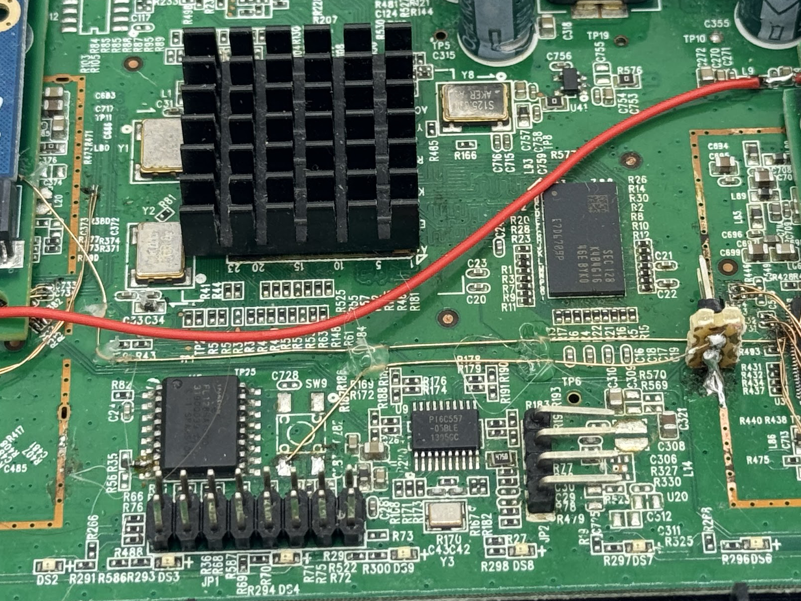
We still couldn’t detect the chip with a CH341, MiniPro TL866 or the Glasgow Interface Explorer. After some electrical troubleshooting we noticed that the CS (chip select) pin of the flash IC was getting pulled up very hard (60+ mA), even with the CPU in reset.
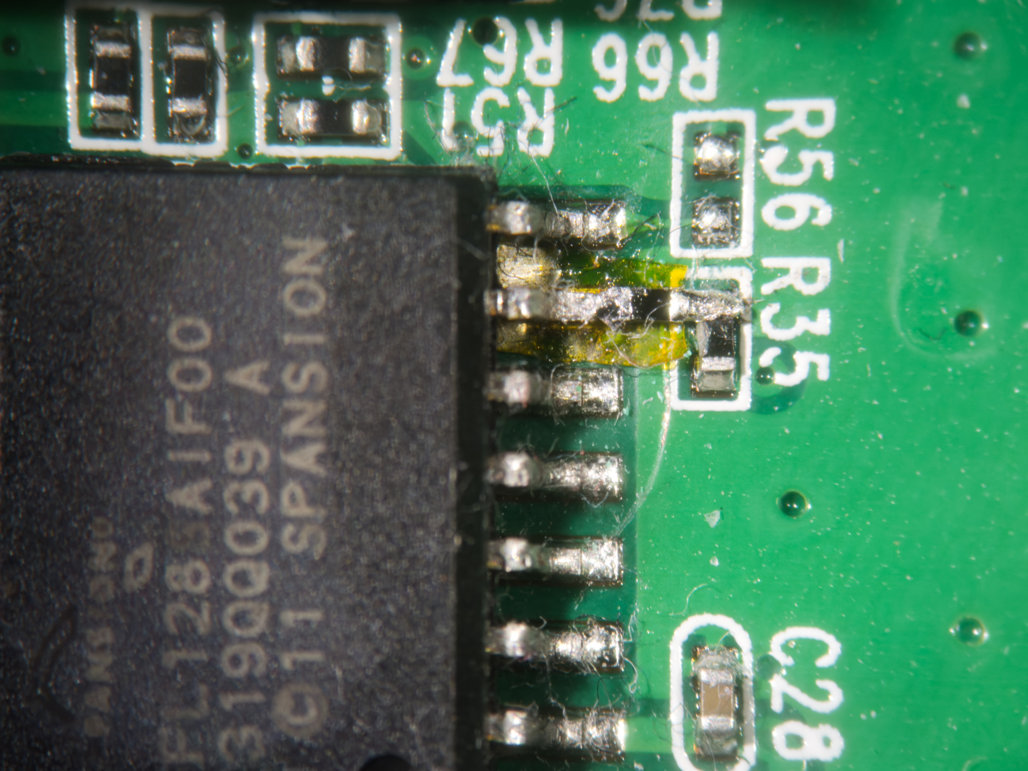
This required some intricate SMD rework. The CS signal was connected to the SOIC-16 footprint directly underneath the pin with a via, so there were no traces to cut. Instead, the pin was lifted, a kapton tape isolator was inserted and the CS pin was reconnected through a 1kOhm SMD resistor to the original signal:
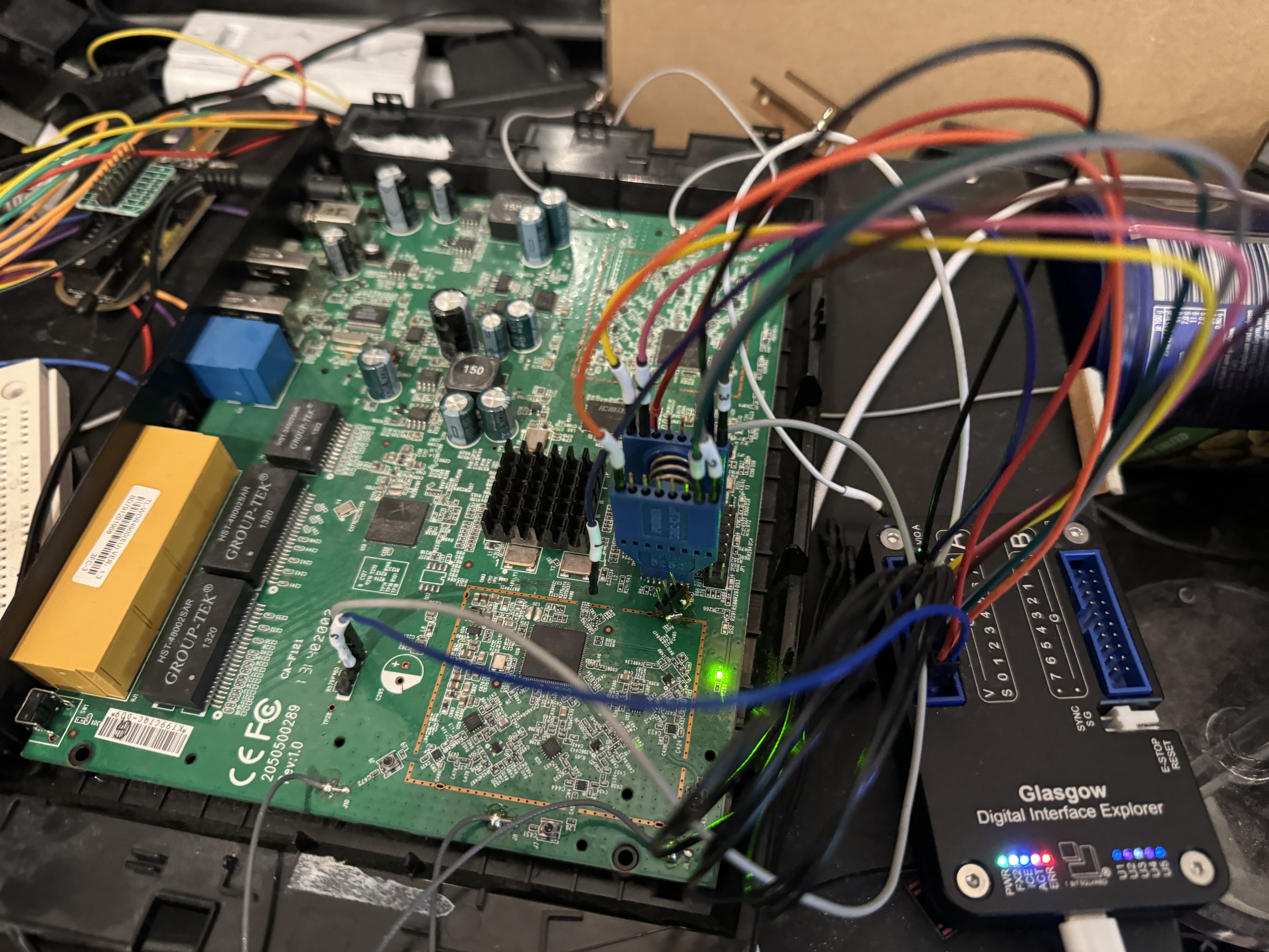
With the help of a Glasgow Interface Explorer and its spi-flashrom applet, we were now able to access the flash IC:
Artisanally handcrafted PPC assembly
After all this trouble flashing the IC, we were greeted with… absolutely nothing. The router was still very dead and didn’t give any signs of life. u-boot (SPL) should announce itself on the UART after start-up.
We tested u-boot’s CONFIG_DEBUG_UART feature, which should use a low-level 16550 UART driver to send some early debug info.
Still no output.
At this point, it was unclear whether code was even being executed. There could be any number of things wrong (L2 init, load/exec addresses, CCSRBAR offset, compiler parameters, broken u-boot, etc.).
Without an external JTAG debugger to inspect the cores state, we were a bit stuck.
Note: Bare-metal C code
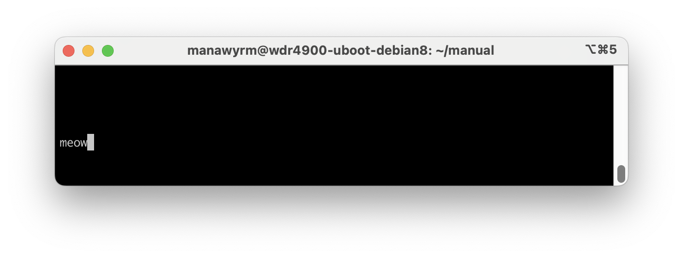
Running C code like this is extremely limited. We currently have neither a heap nor stack setup anywhere. Calling functions or libraries, allocating memory or even just having code too complex to fit into registers would generate machine code which cannot run currently. Simple memory accesses like done below are fine, anything more complex wouldn’t work (without more setup).Writing assembly for PowerPC directly was a bit of a daunting task, instead we wrote a very minimal test.c file to try and get some output:
#define _MMIO_BYTE(mem_addr) (*(volatile unsigned char *)(mem_addr))

int main()
{
    asm volatile ( "nop" );

    _MMIO_BYTE(0xFF704503) = 0x83; // access to baudrate MMIO registers
    _MMIO_BYTE(0xFF704500) = 0xd9; // set baudrate to 115200
    _MMIO_BYTE(0xFF704503) = 0x03; // disable access to baudrate MMIO registers

    _MMIO_BYTE(0xFF704502) = 0x07; // enable FIFO

    asm volatile ( "nop" );

    _MMIO_BYTE(0xFF704500) = 'm';
    _MMIO_BYTE(0xFF704500) = 'e';
    _MMIO_BYTE(0xFF704500) = 'o';
    _MMIO_BYTE(0xFF704500) = 'w';

    while (1) {
        asm volatile ( "nop" );
    }
    return 0;
}
The NOPs aren’t required and were just used as markers to identify the blocks of code in the resulting assembly code.
The linker was instructed to generate code from 0xD0000000 (the start of SRAM):
OUTPUT_ARCH(powerpc)

SECTIONS
{
    IMAGE_TEXT_BASE = 0xD0000000;
    . = IMAGE_TEXT_BASE;
    .text : {
        *(.text*)
    }
[...]
and the code was compiled without any libraries, libc, stdlib to be completely freestanding:
powerpc-linux-gnuspe-gcc -mcpu=8540 -mrelocatable -ffunction-sections -fdata-sections -fPIC -meabi -fno-builtin -ffreestanding -nostdinc -pipe  -ffixed-r2 -Wa,-me500 -msoft-float -mno-string -mno-spe -Wall -Wstrict-prototypes -fno-stack-protector -O0 -c test.c
powerpc-linux-gnuspe-ld -o test.elf -T linker-spi.lds test.o
powerpc-linux-gnuspe-objdump -d test.elf
objdump decodes the register accesses as signed decimal numbers, which results in those strange values like “-144” for the CCSRBAR offset (0xFF70). Reading the hex dump is more helpful in most cases.
Disassembly of section .text:

d0000000 <main>:
d0000000:   94 21 ff f0     stwu    r1,-16(r1)
d0000004:   93 c1 00 08     stw     r30,8(r1)
d0000008:   93 e1 00 0c     stw     r31,12(r1)
d000000c:   7c 3f 0b 78     mr      r31,r1
d0000010:   60 00 00 00     nop
d0000014:   3d 20 ff 70     lis     r9,-144
d0000018:   61 29 45 03     ori     r9,r9,17667
d000001c:   39 40 ff 83     li      r10,-125
d0000020:   99 49 00 00     stb     r10,0(r9)
d0000024:   3d 20 ff 70     lis     r9,-144
d0000028:   61 29 45 00     ori     r9,r9,17664
d000002c:   39 40 ff d9     li      r10,-39
d0000030:   99 49 00 00     stb     r10,0(r9)
d0000034:   3d 20 ff 70     lis     r9,-144
d0000038:   61 29 45 03     ori     r9,r9,17667
d000003c:   39 40 00 03     li      r10,3
d0000040:   99 49 00 00     stb     r10,0(r9)
d0000044:   3d 20 ff 70     lis     r9,-144
d0000048:   61 29 45 02     ori     r9,r9,17666
d000004c:   39 40 00 07     li      r10,7
d0000050:   99 49 00 00     stb     r10,0(r9)
d0000054:   60 00 00 00     nop
d0000058:   3d 20 ff 70     lis     r9,-144
d000005c:   61 29 45 00     ori     r9,r9,17664
d0000060:   39 40 00 6d     li      r10,109
d0000064:   99 49 00 00     stb     r10,0(r9)
d0000068:   3d 20 ff 70     lis     r9,-144
d000006c:   61 29 45 00     ori     r9,r9,17664
d0000070:   39 40 00 65     li      r10,101
d0000074:   99 49 00 00     stb     r10,0(r9)
d0000078:   3d 20 ff 70     lis     r9,-144
d000007c:   61 29 45 00     ori     r9,r9,17664
d0000080:   39 40 00 6f     li      r10,111
d0000084:   99 49 00 00     stb     r10,0(r9)
d0000088:   3d 20 ff 70     lis     r9,-144
d000008c:   61 29 45 00     ori     r9,r9,17664
d0000090:   39 40 00 77     li      r10,119
d0000094:   99 49 00 00     stb     r10,0(r9)
d0000098:   60 00 00 00     nop
d000009c:   60 00 00 00     nop
d00000a0:   4b ff ff fc     b       d000009c <main+0x9c>
After all of this, we were finally given a sign of life from the router:
TLB trouble
We added the debug print assembly to u-boot’s arch/powerpc/cpu/mpc85xx/start.S and then added a little macro:
#define cat_debug(r1_, r2_, v) \
    lis     r1_,-144; \
    ori     r1_,r1_,17664; \
    li      r2_,v; \
    stb     r2_,0(r1_)
This macro accepts 2 registers (which should be unused/scrap) and a single byte, which is printed to the UART. We then littered the early init assembly code of u-boot with debug statements to try and find where the execution stopped.
MMU & TLB 101
The Translation lookaside buffer, in short TLB is a list of mappings from virtual to physical addresses. Usually the TLB will be filled by the OS depending on access privileges and private memory allocations for the currently running task. We’re running a very hardcoded configuration with only a few manually created TLB entries to allow code to run, stack & heap & memory mapped registers to be accessible.The code stopped responding after the TLB init routines. We expected as much, as we probably didn’t have a mapping for the UART MMIO registers anymore. After startup the SoC has a single TLB entry configured, mapping the whole 32bit memory space one-to-one from virtual to identical physical addresses.
We added these hardcoded TLB entries in both AS0 and AS1 to try and keep access to the CCSRBAR:
        create_tlb1_entry 3, \
                0, BOOKE_PAGESZ_4M, \
                0xff700000,  MAS2_I|MAS2_G, \
                0xff700000, MAS3_SX|MAS3_SW|MAS3_SR, \
                0, r6

        create_tlb1_entry 13, \
                1, BOOKE_PAGESZ_4M, \
                0xff700000,  MAS2_I|MAS2_G, \
                0xff700000, MAS3_SX|MAS3_SW|MAS3_SR, \
                0, r6
Much to our surprise, the SPL suddenly sprang to life, started to run properly and output things:
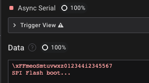
A modern v2024 u-boot seems to be fundamentally broken on P1010-platforms then! We did some more debugging, troubleshooting and followed the code execution down to the C-code init. The SPL tried to load an environment from SPI NOR and crashed while doing so. We just removed the environment functionality as it isn’t needed.
Freescale’s native DDR3 setup code was also running at this point, so we should have a lot of memory to play with now.
Memory testing
Note: Different hardware
We switched to a second WDR4900 (with stock, known-good DDR3 RAM) at this point to develop the testing procedure on a known-good device with working memory.Das U-Boot has a built-in memory testing functionality. As we’re still in SPL (and want to stay there, because a full U-Boot is too big for SRAM), we called the memtest directly in board/freescale/p1010rdb/spl.c:
Apart from the fact that the SPL uses a cut-down version of printf() with limited formatting support (which is why the addresses aren’t displayed and the 8lx format strings are displayed instead), this looked promising.
Let’s generate some errors, then! Grab the finest pair of tweezers and briefly short-out the DDR3 termination resistors:
… no errors reported! Huh?! That can’t be right!
We then also changed the DDR3 timing parameters to absolutely wrong and impossible values to cause some errors. Still, nothing. No errors. What’s going on here?
L1 cache! The P1014’s CPU core has 32 KB of L1 data cache and it’s just caching the correct values for our memtest routine.
We’re testing the L1 cache here, not the actual DDR3 memory!
At this point we tried adding some invalidate_dcache() calls into the testing routine, but this led to lock-ups/crashes. The SPL is very minimal and does not have proper exception handlers yet. It’s possible that the CPU jumped into some exception handler/bus error/hard fault and was stuck there.
As a quick fix, we just disabled caching entirely for the DDR3 TLB entry in arch/powerpc/cpu/mpc85xx/tlb.c:
@@ -261,6 +263,9 @@ uint64_t tlb_map_range(ulong v_addr, phys_addr_t p_addr, uint64_t size,
                wimge = MAS2_I|MAS2_G;
        }

+       // Hack: Force memory coherency, guard and cache-inhibit DDR
+       wimge = MAS2_M|MAS2_I|MAS2_G;
+
        if ((mfspr(SPRN_MMUCFG) & MMUCFG_MAVN) == MMUCFG_MAVN_V1) {
                /* Convert (4^max) kB to (2^max) bytes */
Custom PRBS15 memtest routine
Before we continued on to the potentially broken DRAM, we wanted to have a little bit more robust memory testing routine.
We implemented a small PRBS15 routine, which fills the complete DRAM with pseudo-random, but deterministic test data. The code was inspired by libosmocore’s PRBS15 implementation, but implemented without the osmo_ubit mechanism.
static inline uint32_t prbslong(unsigned int *state)
{
    uint32_t data = 0x00;

    for (int bit = 0; bit < 32; ++bit) {
        int result = *state & 0x1;
        *state >>= 1;
        if (result)
            *state ^= (1<<14) | (1<<13);

        data |= result << bit;
    }

    return data;
}
This function returns the next 32 bits of the PRBS15 sequence for each execution and advances the state variable accordingly.
As long as we start from the same value in state, we get the same data for each call of prbslong().
After filling the DRAM from a fixed state value, we just reset state back to the initial value, read the data back from DRAM and compare it with another call of prbslong().
We are writing much more data than fits into either L1 or L2 cache. If the data being read back is identical with the output of prbslong(), the memory works. By testing several times with different initial state values, we can also randomize the bits in the test data to find stuck bits.
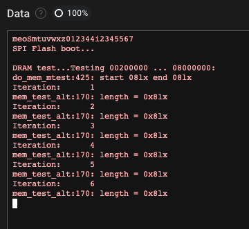
Doing the tweezer test again:
DRAM test...Testing 00200000 ... 08000000:
do_mem_mtest:199: start 08lx end 08lx
Iteration:     1
KittenMemtest PRBS15, writing test pseudo random test sequence
Writing 0x07f00000
Letting data soak for 2sec (auto-refresh test) ...
Reading 0x04700000
Mem error @ 0x0474f940: found 7dacad91, expected 923dc7ad
Mem error @ 0x0474f944: found 88b1e1bd, expected 7dacad91
Mem error @ 0x0474f948: found 6aa76674, expected 88blelbd
Mem error @ 0x0474f94c: found 3c03affa, expected 6aa76674
Mem error @ 0x0474f950: found 5cc0d101, expected 3c03affa
Mem error @ 0x0474f954: found 12fc3950, expected 5cc0d101
Mem error @ 0x0474f958: found 5590cdc1, expected 12fc3950
Mem error @ 0x0474f95c: found d03d3fac, expected 5590cdc1
Reading 0x07500000
Works! We can catch memory errors now.
Memory training REPL
Recompiling U-Boot, connecting the Glasgow, flashing the SPI NOR (and waiting minutes for a full erase, program, verify cycle) and messing with the reset lines was getting annoying quickly.
Big Endian strikes again
microrl worked very well for us in other setups, but it just wouldn’t want to work in the SPL.
Typing characters into the shell just resulted in spaces being printed.
As it turns out, microrl converts the incoming characters (which are passed as an int (32 bit)) to a char* like this:
void microrl_insert_char (microrl_t * pThis, int ch)
{
    if (microrl_insert_text (pThis, (char*)&ch, 1))
This works on little-endian machines (as it points to the LSB), but on our big-endian PowerPC CPU, the character was the MSB (and thus always 0).
We implemented a minimal user interface/shell in the SPL, using microrl:
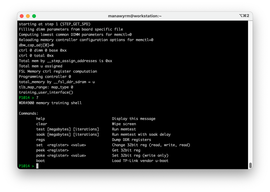
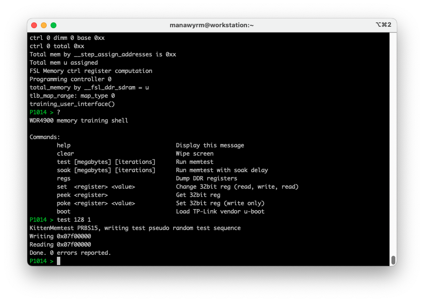
Memory can be tested from the shell using the test command:
Raw memory or register accesses can be done using the peek, poke and set commands:
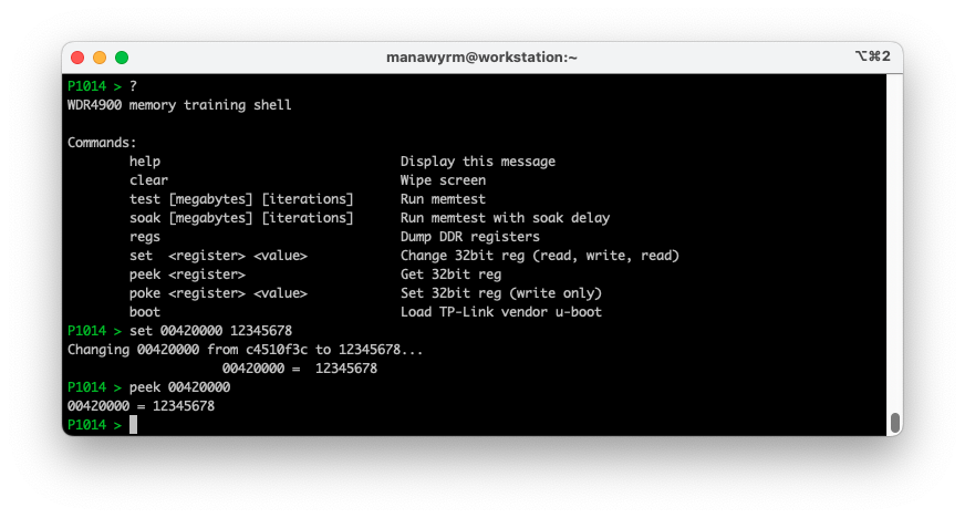
This way, we can tweak the DDR3 controllers MMIO registers quickly (by poking new settings into the MMIO registers) and run a memory test. Rinse and repeat until the memory works.
Memory Swap (Samsung)
Let’s take a look at the memory-swapped router again. We tested various latencies, timings, refresh settings, row/column line configurations, but just couldn’t get the ICMAX memory to hold any data at all.
So at this point, the problem could either be caused by bad soldering or a defective/fake chip.
The router went back on the hot plate and the memory was swapped again, this time with a nice, genuine
Samsung K4B4G1646E 4Gbit/512MByte x16 chip: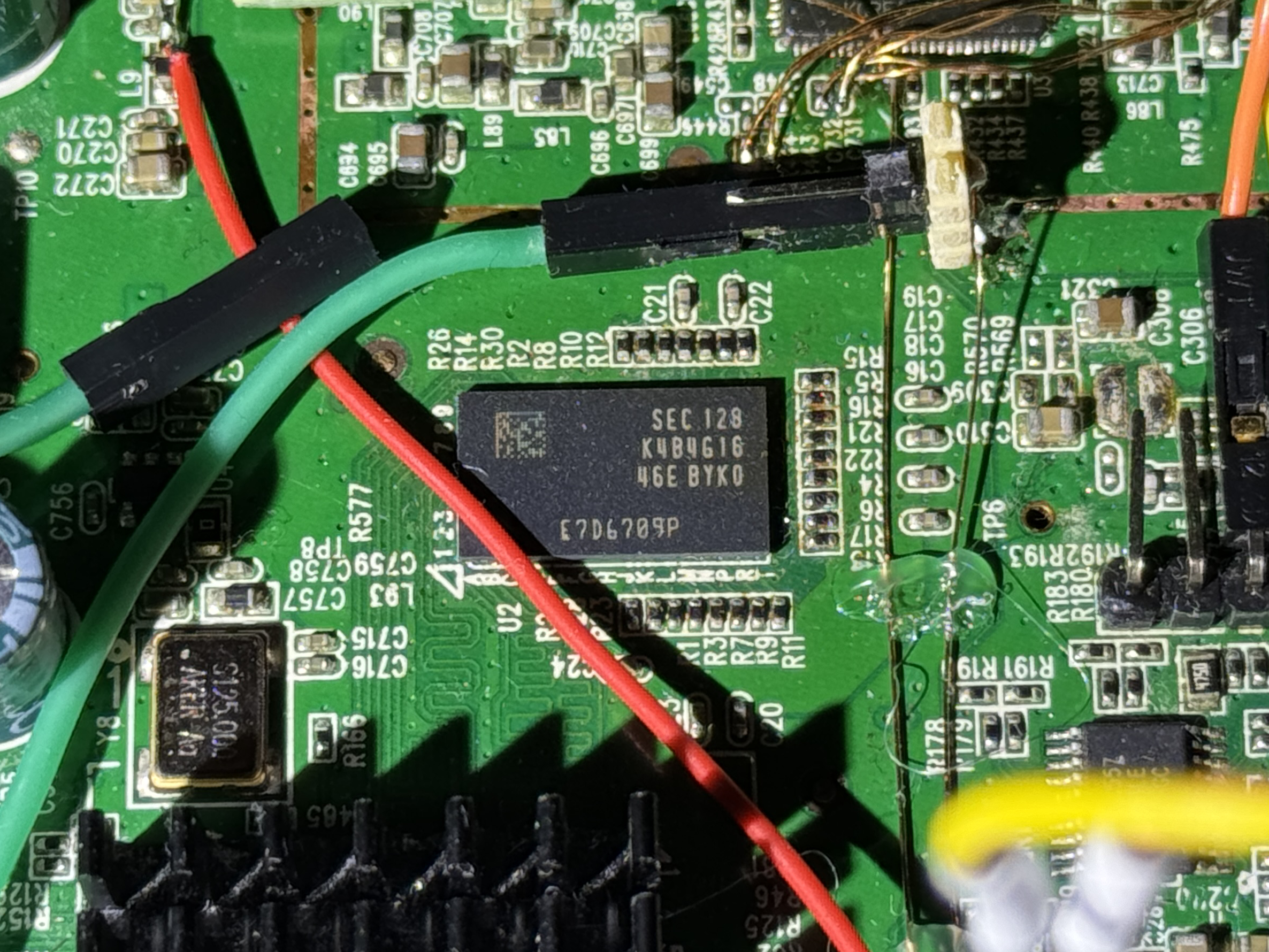
Moment of truth:
DRAM test...Testing 00200000 ... 08000000:
do_mem_mtest:199: start 08lx end 08lx
Iteration:     1
KittenMemtest PRBS15, writing test pseudo random test sequence
Writing 0x07f00000
Letting data soak for 2sec (auto-refresh test) ...
Reading 0x07f00000
Tested 1 iteration(s) with 0 errors.
\o/
The Samsung memory works (or at least the first 128 MiB being tested)!
Memory Aliasing
Let’s just set the Linux device tree to 512 MiB of RAM and boot right into the OS!
    memory {
-       reg = <0x0 0x0 0x0 0x8000000>;
+       reg = <0x0 0x0 0x0 0x20000000>;
    };
The memory training UI was extended with a boot command, which loads the stock TP-Link U-Boot into DRAM (at 0x10000000, where it always is) and jumps to it. We can then just load a Linux kernel via TFTP and run it.
Linux started to boot and then just crashed in the wildest spots with very strange kernel panics. What’s going on here?
Let’s take a step back and use the REPL again.
Ran test 512 1 to test 512 MiB of RAM and… tons of memory errors right from the start.
Right from address 0x00000000, the content was wrong. Testing 128 MiB worked fine, 256 MiB as well.
Testing 257 MiB with test 257 1 did not. Touching any memory above 256 MiB caused the data at the start of memory to get corrupted.
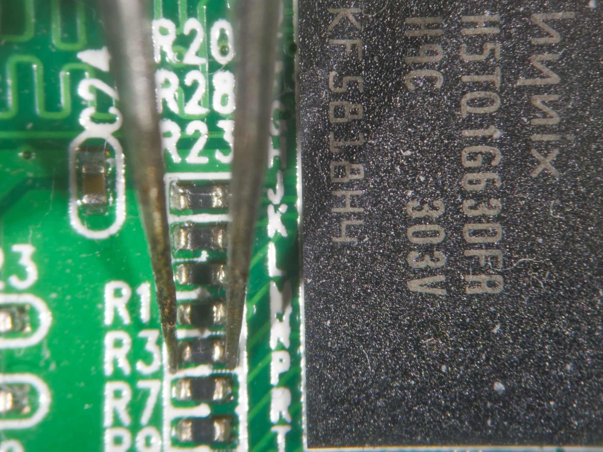
We looked at a photo of the pads below the DDR3 IC (while it was being replaced):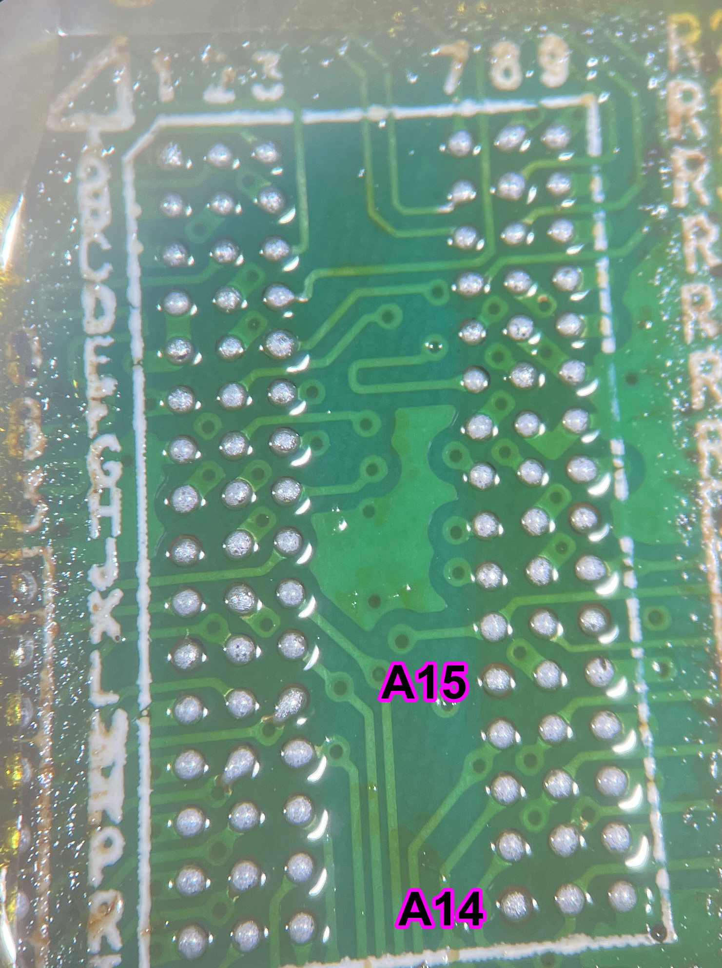
… *sigh*
The upper address bits A14 and A15, required to address 512 MiB and 1 GiB of RAM aren’t connected on TP-Link’s PCB.
The P1014 SoC has the A14 and A15 pins, but they aren’t connected anywhere.
This was a bit disheartening, as it meant the maximum memory supported by the TL-WDR4900v1 was 256 MiB.
We changed the configuration of U-Boot and the Linux kernel accordingly and everything worked fine:
    memory {
-       reg = <0x0 0x0 0x0 0x20000000>;
+       reg = <0x0 0x0 0x0 0x10000000>;
    };
Supporting any more memory would require some pretty invasive SMD surgery, involving the removal & reballing of the BGA CPU and running additional traces along the PCB. Not something we’d like to focus on right now.
Memory & CPU clock speed
Over on forum.openwrt.org, user dabyd64 posted some very interesting notes about the strapping pins of the CPU:
(Image credit: dabyd64)
The memory speed can be changed from 667 MHz (1333 MT/s) to 800 MHz (1600 MT/s) and the CPU speed can be increased to up to 1.4 GHz (with over-volting) from the stock 800 MHz!
We modified our router to run at a DRAM speed of 800 MHz (1600 MT/s) and a CPU speed of 1200 MHz.
Re-tested the memory after the modification and everything looked fine!
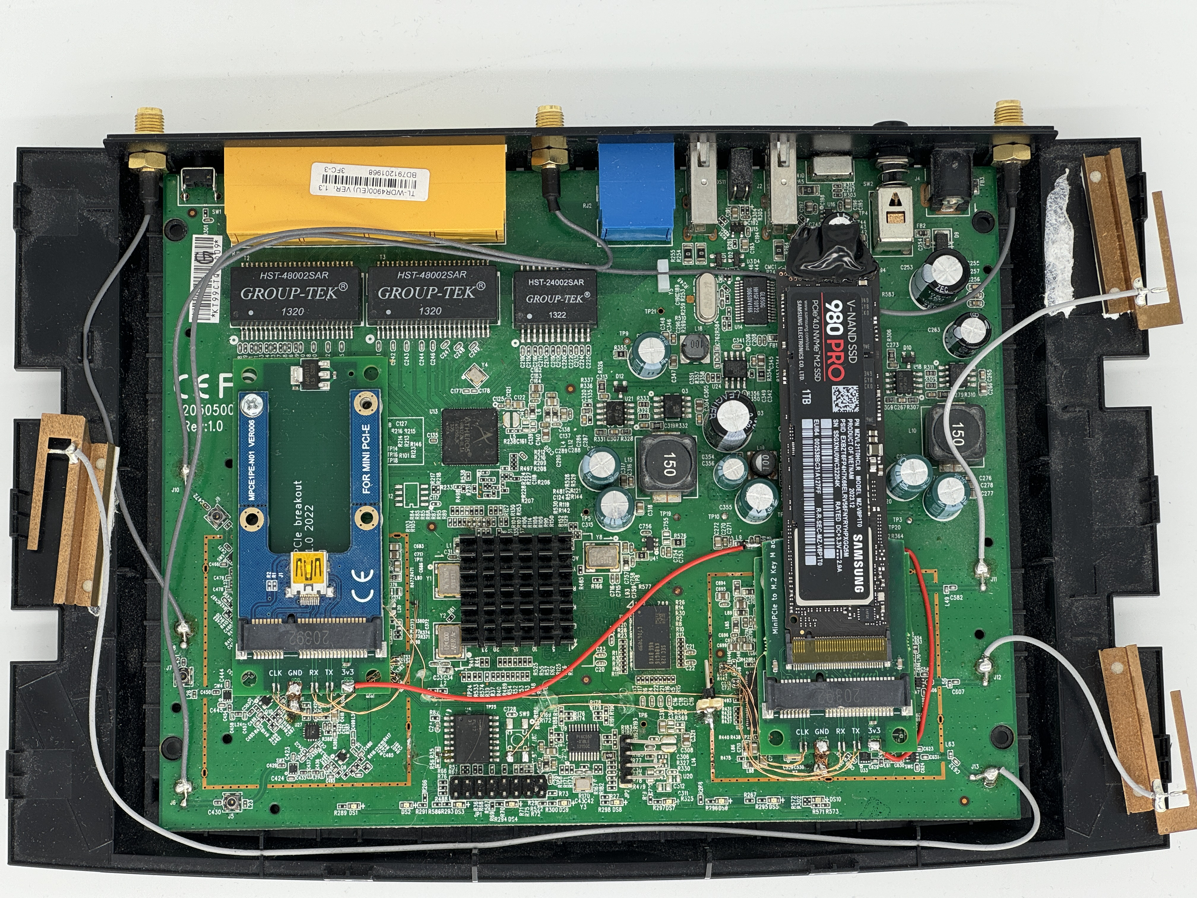
PCIe & NVMe slots
Similar to the original mod, the PCIe traces from the SoC to the WiFi chips were cut and re-routed to little miniPCIe breakout boards. This time, both WiFi chains (2.4 GHz and 5 GHz) were cut and connected to 2 separate miniPCIe slots.
First miniPCIe slot (including a miniPCIe -> M.2 M-key adapter):
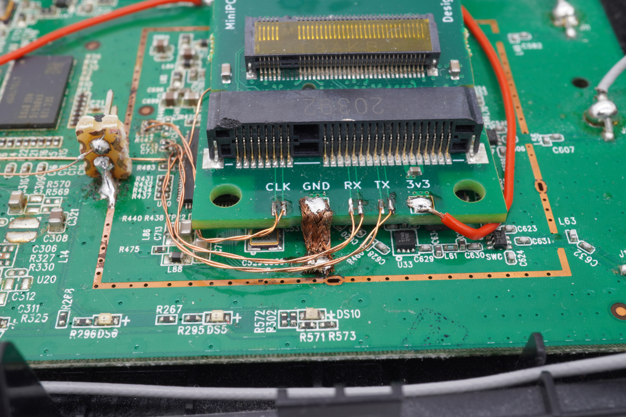
Second miniPCIe slot (including the miniPCIe -> miniUSB 3.1 (sic!) breakout PCB):
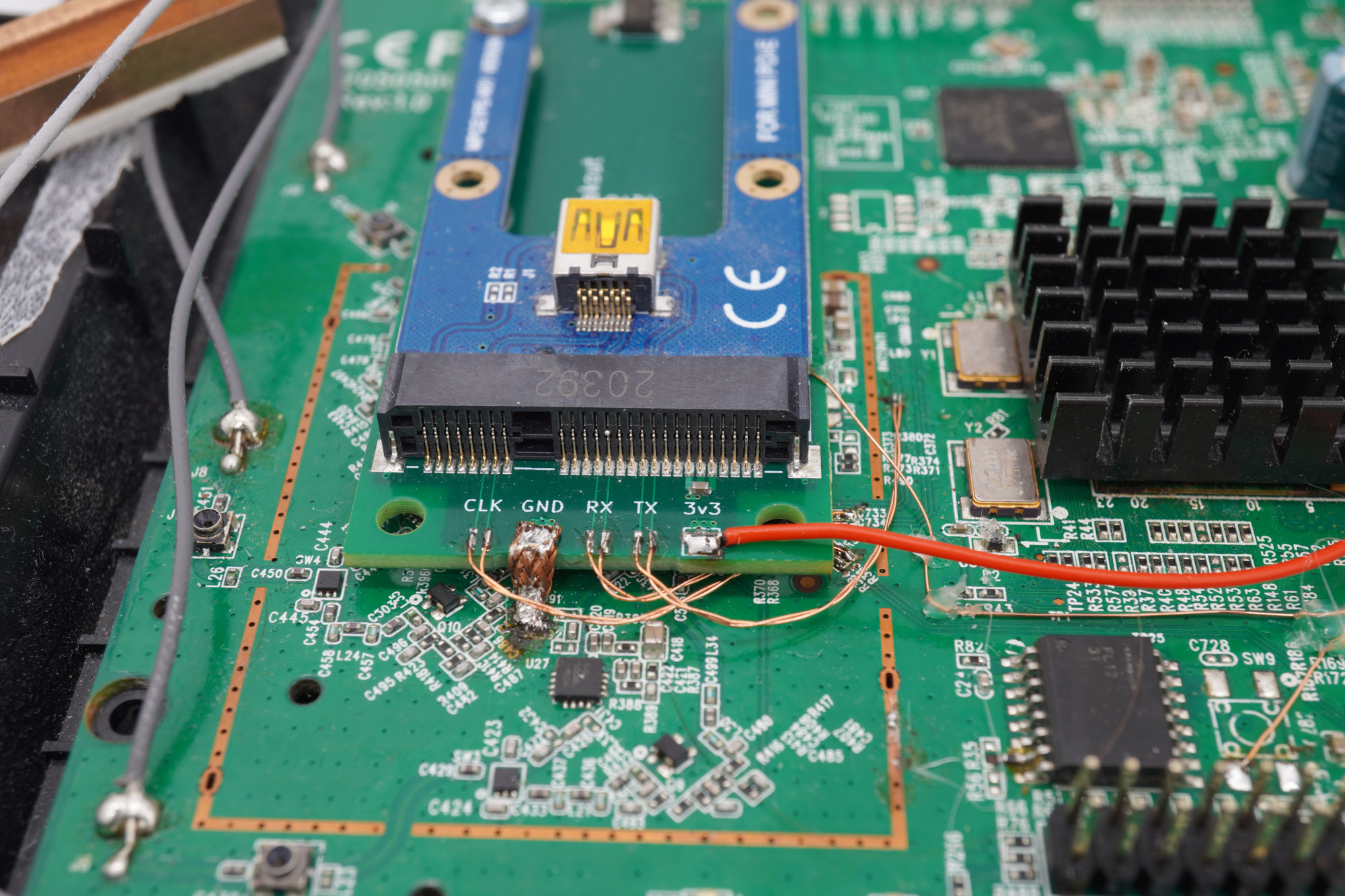
This allows for both the Radeon GPU and an internal NVMe SSD to be connected simultaneously.
Benchmarks (dd/md5sum)
Generating the MD5 checksum of 1GiB read from /dev/zero was the benchmark used by dabyd64 in the overclocking post. We used the same test to keep our results comparable.
Interestingly, our (stock) results were already much better.
dabyd64’s test at 800 MHz took 26s (39.4MB/s), while ours only took 14s (76.0 MB/s).
The most likely explanation is either the newer Linux kernel or the full Debian/GNU userland (instead of Busybox).
800 MHz CPU, 1333 MT/s, without L2 cache
root@gaming-router:~# time dd if=/dev/zero bs=1M count=1024 | md5sum
1073741824 bytes (1.1 GB, 1.0 GiB) copied, 17.421 s, 61.6 MB/s
real    0m17.451s
800 MHz CPU, 1333 MT/s, with L2 cache (stock configuration from TP-Link):
root@gaming-router:~# time dd if=/dev/zero bs=1M count=1024 | md5sum
1073741824 bytes (1.1 GB, 1.0 GiB) copied, 14.1219 s, 76.0 MB/s
real    0m14.154s
1200 MHz CPU, 1600 MT/s, with L2 cache:
root@gaming-router:~# time dd if=/dev/zero bs=1M count=1024 | md5sum
1073741824 bytes (1.1 GB, 1.0 GiB) copied, 10.4496 s, 103 MB/s
real    0m10.460s
Testing performance
With the additional RAM, Swap-on-NVMe (and the SSDs own DRAM) and the higher CPU and RAM speed, the game performance in GTA Vice City was improved significantly.
The performance felt a bit… odd, though. The game was a bit stuttery and even in low-RAM-usage areas (like indoors in a building), the game performance felt worse than before.
Some more custom code was written to test the memory performance with different transfer sizes (to stay in L1, then L2 cache and finally hit DRAM).
Performance results
In this memory speed vs. transfer size chart, you can clearly see the 3 different memory tiers being available.
The L1 cache is clocked by the CPU clock, which means that the L1 throughput has improved by ~50% to over 4.5 GByte/s with our CPU overclock!
L2 cache throughput increased slightly to about 1.6 GByte/s, while the extra DRAM speed “only” accounted for an additional 100 MByte/s of throughput (still a 13% increase, not bad for moving a resistor!).
Re-enabling L2 cache
Because we enabled L2-as-SRAM, ran our custom SPL there and then jumped to the vendor U-Boot, L2 cache was still disabled! This is very detrimental to the system performance, of course. Neither the vendor U-Boot, nor Linux double checked the configuration and re-enabled L2.
One possible solution would be to write a small shim, which is loaded into DRAM and then executed, enables L2 and then jumps to the actual payload (U-Boot). As we’re already using a custom Linux kernel, the much easier solution is to extend Linux’ board support file for the WDR4900.
In arch/powerpc/platforms/85xx/tl_wdr4900_v1.c, we added a routine to re-enable the L2 cache:
static void __init configure_l2_cache(void __iomem *l2_base)
{
    volatile uint32_t tmp;

    asm volatile("msync; isync");
    tmp = in_be32(l2_base);
    printk(KERN_INFO "TL-WDR4900 v1: L2_Cache_L2CTRL: 0x%08x\n", tmp);

    /* Step 1, disable SRAM */
    printk(KERN_INFO "TL-WDR4900 v1: Disabling SRAM...\n");
    asm volatile("msync; isync");
    out_be32(l2_base, 0x10000000);
    tmp = in_be32(l2_base);
    asm volatile("msync; isync");

    /* Step 2, enable L2 cache */
    printk(KERN_INFO "TL-WDR4900 v1: Enabling L2 cache...\n");
    asm volatile("msync; isync");
    out_be32(l2_base, 0xb0000000);
    tmp = in_be32(l2_base);
    asm volatile("msync; isync");

    printk(KERN_INFO "TL-WDR4900 v1: L2_Cache_L2CTRL: 0x%08x\n", tmp);
}
JTAG adapter
Pretty much at the end of this journey, we were lent an Abatron BDI2000 JTAG debugger. This device can be flashed with the MPC85xx firmware and will then expose a GDB server over 10Base-T Ethernet. It allows for full control over the CPU core, viewing/changing registers, reading/writing to memory, starting/stopping the CPU, setting breakpoints, etc.
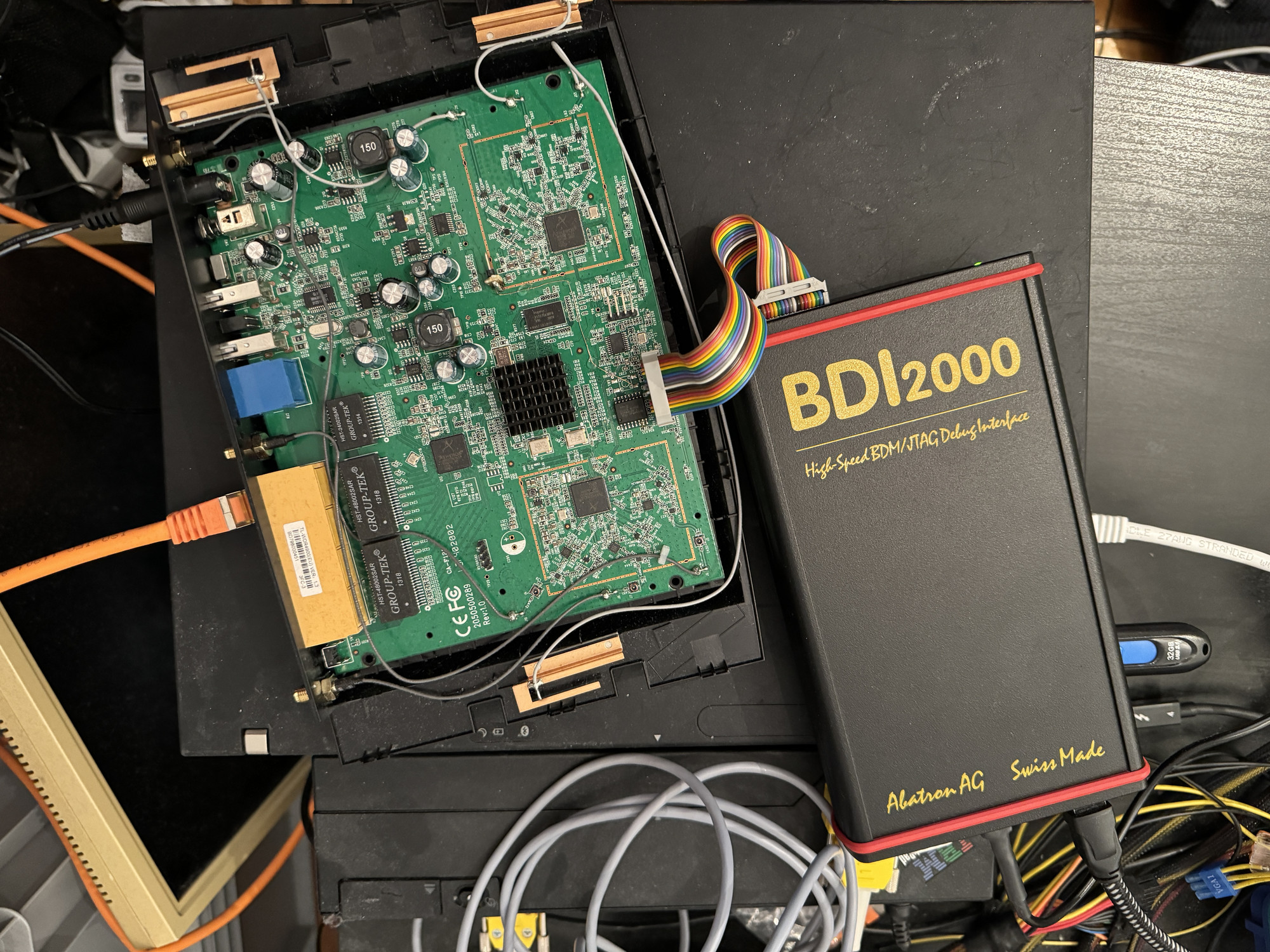
Pressing Ctrl-C in gdb halts the CPU and we can run bt full while the CPU is waiting for input in the memory training REPL to see exactly that on the stack: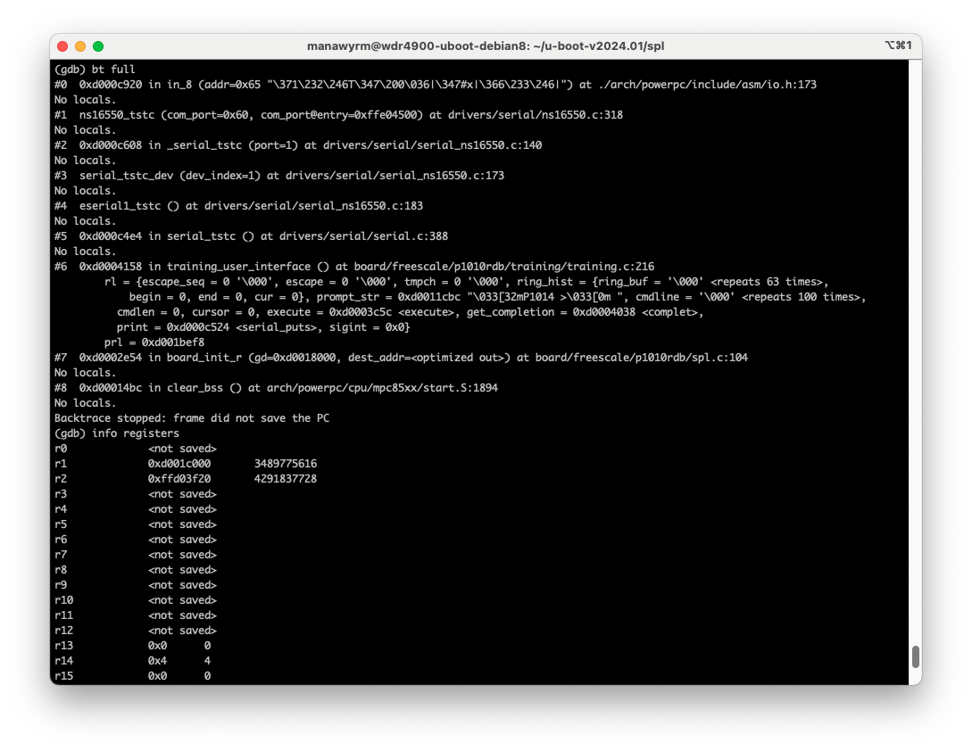
This also significantly improves the development experience by shortening the test cycle. Code can be loaded directly into SRAM, without having to deal with SPI flash, boot-format or anything related.
The debugger will be used to clean up the changes to the SPL and probably debug some other long-standing platform issues we encountered over the years.
Final result
Changes:
- 256 MB RAM (instead of 128 MB RAM)
- 1200 MHz CPU (from 800 MHz CPU)
- 1600 MT/s RAM (from 1333 MT/s RAM)
- Second PCIe slot / NVMe storage (instead of USB 2.0 SSD)